Monday, 6th July 2026

Khabor Wala Desk
Published: 22nd February 2026, 8:32 AM
In today’s technology-driven world, the country that commands control over semiconductor “chips” invariably holds a decisive technological advantage. From artificial intelligence and electric vehicles to smartphones and advanced defence systems, semiconductors sit at the heart of nearly every modern innovation. Recent industry forecasts suggest that the global semiconductor market is on course to approach US$1 trillion within the next few years. Yet, paradoxically, the sector faces a pronounced shortage of skilled professionals worldwide.
Against this backdrop, Bangladesh must think strategically. Drawing upon both research and industrial experience, it is evident that the country can carve out a position in this high-value industry—provided it chooses the right entry points and invests wisely in human capital.
In my experience, three elements are indispensable for a successful career in semiconductors: a strong academic foundation, clarity of direction, and hands-on practical experience.
First and foremost, students should select a clear “track” rather than attempting to master everything simultaneously. Potential pathways include:
Digital VLSI design and verification
Physical design and timing analysis
Analogue and mixed-signal design
Power electronics
At present, verification engineering is particularly in demand globally, making it an accessible entry point into the semiconductor industry for many graduates.
A firm grasp of semiconductor physics, CMOS fundamentals, and VLSI design principles is essential. Complementary technical skills—such as Python programming and Linux proficiency—significantly enhance employability. Equally important is practical exposure: familiarity with Verilog/SystemVerilog, open-source PDKs and design flows, and version control systems such as Git is now indispensable.
Notably, open-source tools have democratised chip design. Students can now complete small-scale chip design flows independently—something that was virtually impossible a decade ago. In this field, project experience often outweighs CGPA. Designing your own RTL block, generating simulation reports, documenting your workflow, and publishing projects on GitHub can provide a distinct advantage when applying for overseas study or employment.
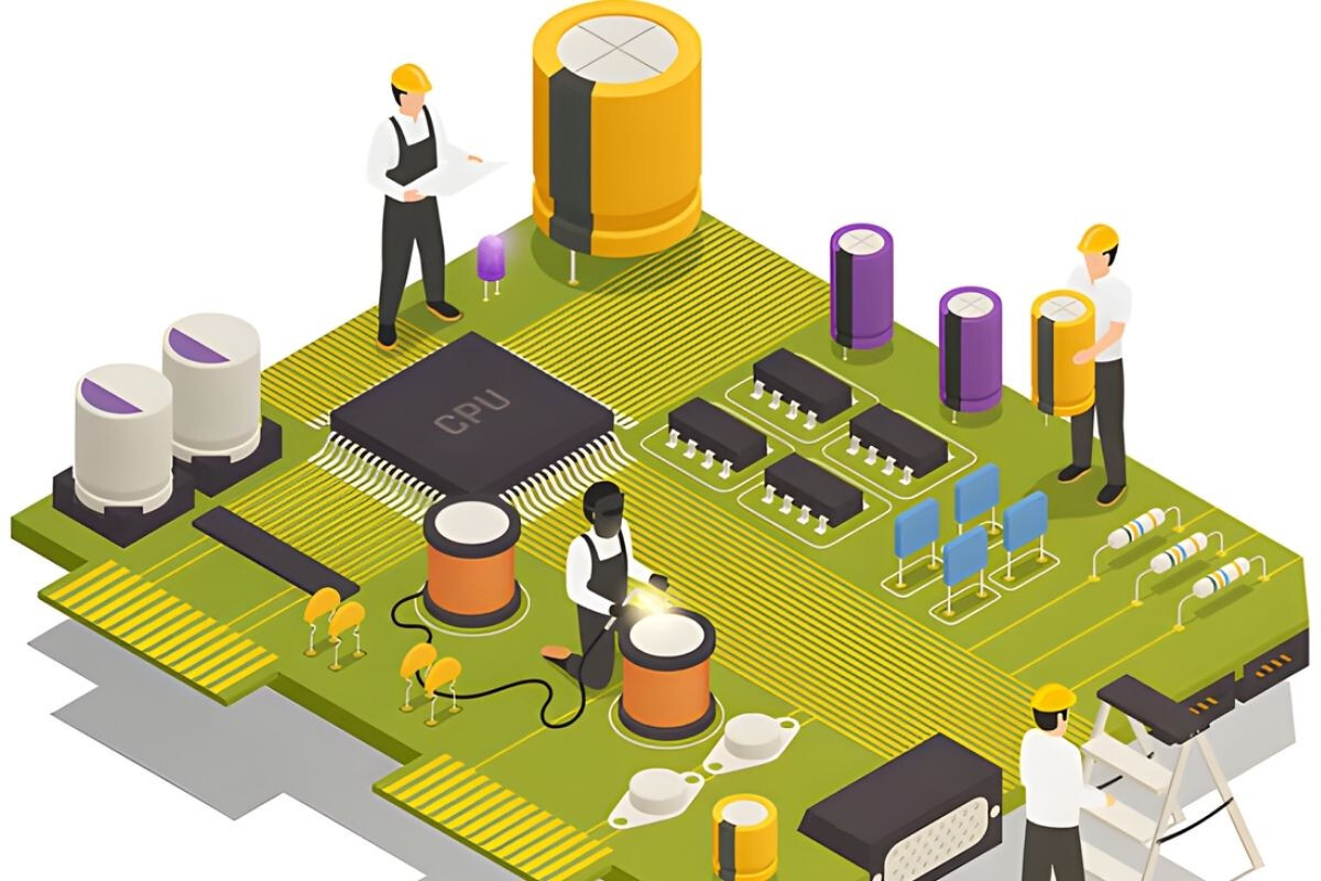
The semiconductor value chain is multifaceted and interconnected. It can broadly be divided into four principal layers, though Bangladesh’s opportunities differ across them.
| Segment | Core Activities | Investment Intensity | Bangladesh’s Near-Term Potential |
|---|---|---|---|
| Fabless Chip Design | RTL, verification, physical design, DFT, analogue/mixed-signal | Moderate | High |
| Testing & Packaging (OSAT/ATP) | Assembly, testing, packaging | Moderate | High |
| Device & Process Engineering | Wafer fabrication, lithography, etching, deposition | Very High (billions USD) | Low (long-term) |
| Equipment & Materials | Lithography systems, speciality gases, wafers | Extremely High | Very Limited |
This is the most realistic and immediately accessible segment for Bangladesh. It involves integrated circuit (IC) design rather than fabrication. Start-ups and design houses can operate without building costly fabrication plants. With a well-trained workforce, Bangladesh could develop competitive design services and system-level solutions.
Outsourced Semiconductor Assembly and Test (OSAT), also known as Assembly, Test and Packaging (ATP), represents a practical entry point for developing economies. Compared to fabrication plants, capital requirements are significantly lower. This segment can generate substantial employment, particularly for electrical, mechanical, and industrial engineers.
This fabrication-centred domain encompasses silicon wafer production, photolithography, ion implantation, etching, and deposition—all within highly controlled cleanroom environments. Establishing a modern fabrication facility demands multi-billion-dollar investment, making it a long-term ambition for Bangladesh.
Advanced machinery—such as lithography systems and plasma etching tools—and specialised materials, including photoresists and high-grade silicon wafers, underpin the industry. Bangladesh’s current industrial base is not yet prepared for this capital- and technology-intensive segment.
Establishing a full-scale commercial fabrication plant is a long-term and extraordinarily expensive endeavour. Taiwan’s rise to global prominence in semiconductors was the result of decades of sustained investment and strong state backing. Bangladesh must therefore prioritise human capital development.
Universities should expand research laboratories, pilot lines, and small-scale prototyping facilities—not merely as academic exercises but as dynamic hubs linked closely with industry. Emerging semiconductor design initiatives within the country should collaborate actively with academia. Structured internships, joint research programmes, and industry-driven capstone projects can cultivate a pipeline of skilled engineers.
Ultimately, Bangladesh’s semiconductor future will depend not on infrastructure alone, but on the expertise and ingenuity of its engineers. With strategic planning and sustained commitment, the country can secure a meaningful foothold in one of the world’s most critical industries.


Comments